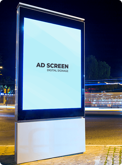
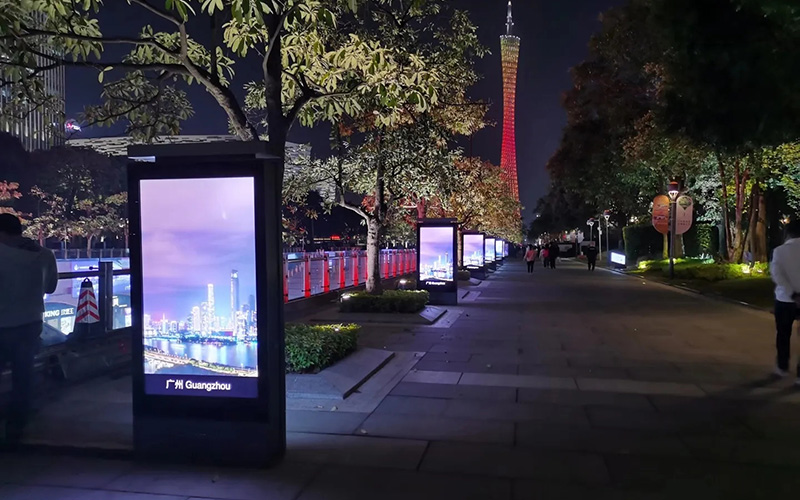
high brightness window LCD screen


Window Facing High Brightness LCD Display widely used in indoor situations,such as restaurants,shops,super markets,airport and subway stations. Normally the indoor advertising display uses LCD product from 32 inch to 86 inch. Floor standing and wall mounted are both available. We can add a touch panel if you need the interact function, such as search the locations and destinations in the shopping mall. It makes people’s life more interesting and intelligent.


Now most of the digital signage’s brightness is about 350-500 nits,it’s difficult to meet the commercial needs . Simultaneously the buildings use high brightness lighting sources ,shopping malls and airport terminals use transparent roofs, those make the low brightness digital advertising display looks very badly.

high brightness window LCD screen

If the lcd digital advertising display looks badly when facing to strong lighting sources,then it’s time to upgrade the digital signage to a high brightness indoor advertising display , which supports 1500 cd/m2 or more. Its screen is bright enough to show the advertised product clearly.It’s very helpful to promote products.

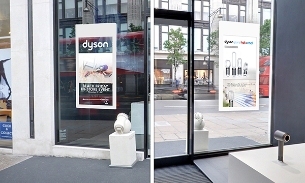
The high brightness lcd digital signage is more and more widely used everywhere,specially in restaurants and shop windows. Most of the shop windows are facing to outside,where is very bright. So it’s necessary to install an high brightness window advertising display, it helps you to show the products to the people who go pass your window.

high brightness window LCD screen

Now the brightness of digital window display is up to 4000cd/m2,the high brightness digital display helps you to solve the reflection problem because of the dark advertising display.

The high brightness digital signage normally use the industrial grade panel from LG or BOE. And it supports auto dimming function, which works according to the ambient light. That helps to cut down the power consumption.

What’ more,we’re very experienced to adjust the contrast ratio and color gamut, that’s very important for a high definition LCD screen.

The high bright digital signage supports to be spliced,within 5mm gaps, which is suitable for a large area window advertising display. get more products details at www.cnlcdisplay.com.


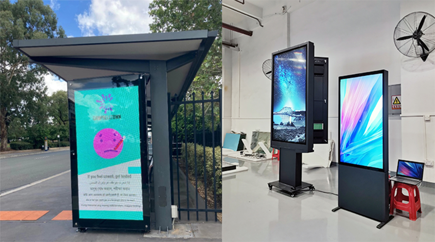
outdoor LCD digital signage

With the development of economy and the progress of technology, LCD outdoor digital signage has gradually become an important and indispensable equipment in urban construction. With the advantages of high definition, wide angle view and good brightness, LCD outdoor digital signage is widely used in public transportation, advertising and weather forecasting, providing important information services for urban life and operation.


First of all, outdoor LCD digital signage has the characteristics of high definition. It adopts imported raw materials and high-end equipment, and carries out a variety of high-precision processing in the production process, which can present clearer and more delicate images, not only presenting good effects, but also long life span, and can withstand harsh climatic and environmental conditions.


outdoor LCD digital signage

In addition, the LCD outdoor digital signage has the feature of wide angle view. This digital signage adopts the latest LCD panels with a wider field of view, allowing more angles to be used to view information. In the process of outdoor information distribution, the wider the field of view area, the more it can attract people's attention. By using LCD outdoor digital signage, information will be conveyed more quickly and accurately. 

Another advantage of LCD outdoor digital signage is its high brightness. It uses LED backlight technology, and its brightness is higher than that of ordinary LCD LCD screens. By adjusting the brightness under stronger sunlight, the outdoor digital signage can maintain a brighter display, thus enabling people to understand and get the message more clearly without the interference of sunlight. 


In a word, LCD outdoor digital signage is a kind of digital display device with high definition and high brightness and wide angle view, which is suitable for advertising, weather forecast, public transportation and other fields. As urbanization accelerates and the demand for information services continues to escalate, LCD outdoor digital signage will certainly play an increasingly important role and bring higher quality displays and services.


In fast-paced days, outdoor advertisement has become an important way for companies to attract attention. However, traditional outdoor LCD advertising display often appear dim due to the impact of sunlight and cannot effectively convey information. But now, we are proud to launch a aluminum outdoor high-brightness LCD display, with its extremely high brightness and visibility under sunlight, let your brand shines outdoors.


high-brightness LCD display


The high brightness outdoor LCD display from CNLC adopts advanced high brightness backlight technology, ensuring that it can keep a bright and clear images(or videos) under strong sunlight. At the same time, our product is equipped with an ultra efficient heat dissipation system and pre heating system. No matter in summer or winter, our LCD display can work stably and without impact by temperature fluctuations. Whether the shops are along the street, in waiting area at a station or a stadium,our outdoor LCD display effortlessly catch the eye of the audience.


 high-brightness LCD display


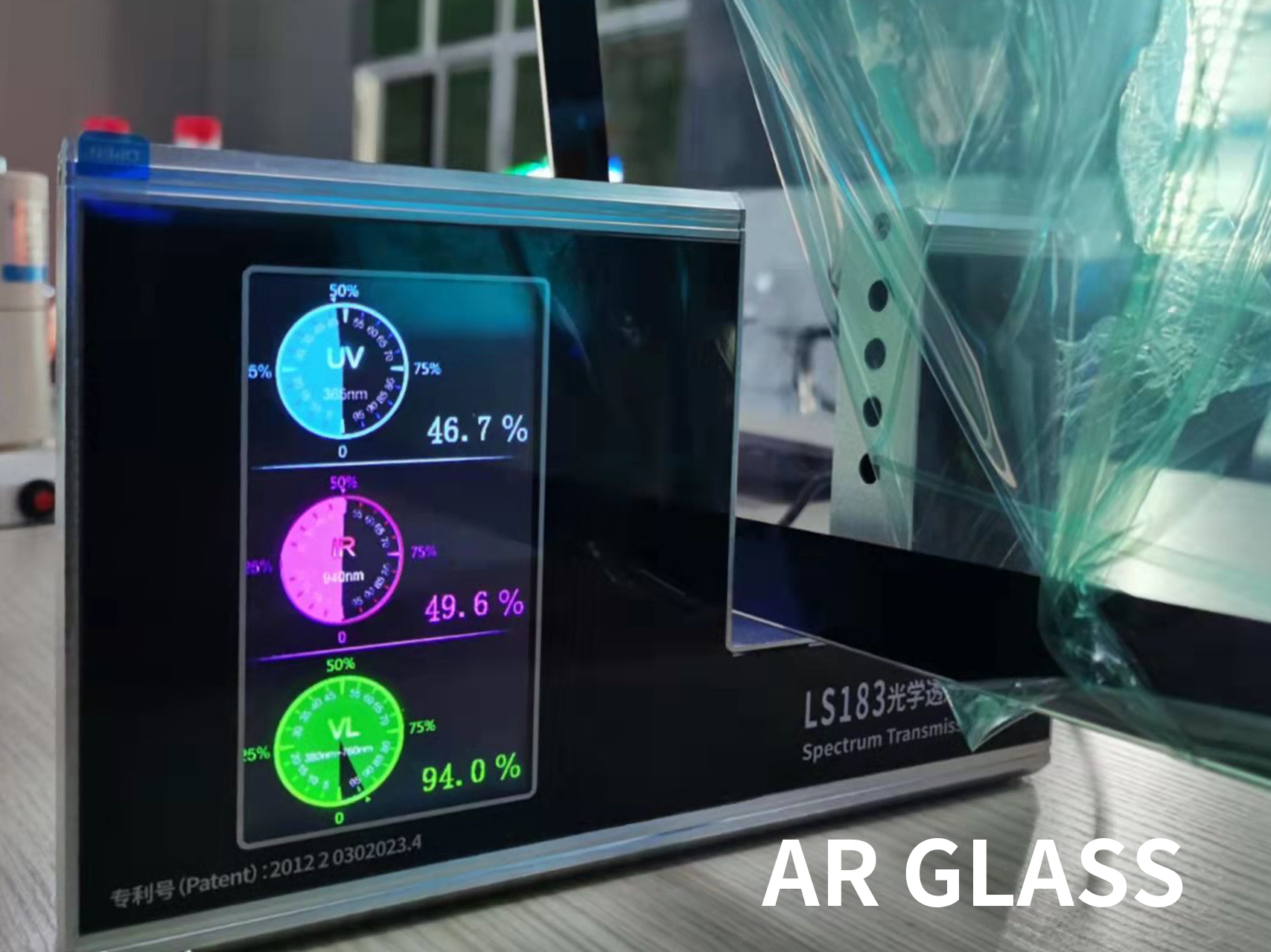
In order to solve the problem of reflection and interference in outdoor environment, the high brightness outdoor LCD display is equipped with professional anti-reflection coating and anti light interference technology. These technologies can effectively reduce the reflection of sunlight, provide better visibility for the LCD screen, ensure that the media contents are clearly visible, and facing direct sunlight, the customers can easily capture all details of advertised product.

LCD digital signage


Electronic lcd signage is undoubtedly an ever more popular approach for enterprises. Throughout the years, the technology has progressed to make modern-day and entertaining displays which you can use for a variety of uses.


Electronic LCD signage is becoming more and more well-known for a number of reasons. First, it gives a simple way to obtain messages to customers quickly and efficiently. Create engaging visuals, videos and also other content material that immediately seize the viewer's attention. This assists interact with individuals while also offering all of them with the information they need.


Electronic lcd signage is starting to become ever more popular like a a lot more vibrant, adaptable and cost-effective option for enterprises and agencies that are looking to convey with their customers and followers:

 Electronic lcd signage


1. Enhancing brand image: LCD digital signage can display a company's brand image, promotional slogans and product information, enhancing the visibility and reputation of corporate brands.


2. Clear display effect: LCD digital signage has clear display effect and bright colors, which can attract customers' attention and increase sales.


3. Remote control: LCD digital signage can be maintained and managed through remote control software, saving labor costs and facilitating regular updates and maintenance.


4. High flexibility: LCD digital signage has various styles, which can meet different occasions and needs, and at the same time, it can flexibly adjust the content and layout according to the actual situation.


5. Sustainable energy saving: LCD digital signage adopts LED backlight, which has low power consumption, low heat generation and long service life, suitable for long-term use. And compared with traditional poster advertising, LCD digital signage can be recycled, reducing the impact on the environment

Polishing terrazzo floors goes beyond simply creating a shiny surface; it is a scientifically intricate procedure that involves understanding material properties, abrasives, friction, and chemical reactions. Terrazzo is a composite material made up of marble, granite, quartz, and glass chips set in cement or resin binders. Each of these components reacts differently during the polishing process, making it a fascinating subject for exploring how surface science affects both the appearance and longevity of the floor.


The hardness of the chips and binders is crucial in selecting the right abrasives and polishing methods. The Mohs hardness scale, which assesses a material’s resistance to scratching, is commonly used to analyze the components of terrazzo. Diamond grinding tools, which have a high Mohs rating, are vital for polishing terrazzo because they can effectively cut and refine a mix of hard and softer materials. This variation in hardness allows diamond abrasives to selectively polish tougher surfaces like marble and granite while quickly smoothing softer elements, resulting in a uniform and balanced finish.


Friction and heat are also important factors in the terrazzo polishing process. As polishing progresses, each abrasive grit increases friction, generating heat that slightly softens the binder. This controlled heating helps to close microscopic pores and imperfections on the floor, enhancing its smoothness and reflective quality. However, too much heat can lead to thermal damage, particularly in resin-based terrazzo, so it is essential to manage friction and temperature to avoid problems like discoloration or weakening of the binder.


terrazzo floor polishing


The principles of the light reflection and refraction contribute an optical dimension to terrazzo floor polishing. A polished terrazzo floor appears glossy because the surface roughness is minimized to a point that allows fro specular reflection, where light bounces off evenly, creating a mirror-like effect. Achieving this uniform reflectivity involves a careful balance of micro-abrasion and polishing. As the surface is refined at a microscopic level, each aggregate chip reflects light in harmony with the others, showcasing the unique mosaic pattern of the terrazzo and enhancing its visual appeal.


TransGrind Diamond Tooling, a professional manufacturer and supplier of premium diamond grinding tools, brings science-driven innovation to terrazzo floor polishing. Our high-performance, durable, and precise tools are crafted to handle the unique challenges of terrazzo’s composite materials, ensuring optimal results in grinding and polishing. To explore our wide range of specialized products designed for exceptional results, visit us at www.transgrindtools.com.

The environment of an electron microscopy lab does not directly impact the electron microscope itself but rather affects the imaging quality and overall performance of the microscope. During the operation of an electron microscope, the fine electron beam needs to travel in a high vacuum environment, covering a distance of 0.7 meters (for Scanning Electron Microscope) to over 2 meters (for Transmission Electron Microscope). Along the path, external factors such as magnetic fields, ground vibrations, noise in the air, and airflows can cause the electron beam to deviate from its intended path, leading to a degradation in imaging quality. Therefore, specific requirements need to be met for the surrounding environment.


Passive low-frequency electromagnetic shielding primarily involves two methods, which differ in the shielding material used: one method uses high-permeability materials (such as steel, silicon steel, and mu-metal alloys), and the other method uses high-conductivity materials (such as copper and aluminum). Although the working principles of these two methods are different, they both achieve effective reduction of environmental magnetic fields.


A. The high-permeability material method, also known as the magnetic circuit diversion method, works by enclosing a finite space (Region A) with high-permeability materials. When the environmental magnetic field strength is Ho, the magnetic reluctance of the high-permeability material is much smaller than that of air (common Q195 steel has a permeability of 4000, silicon steel ranges from 8000 to 12000, mu-metal alloys have a permeability of 24000, while air has an approximate value of 1). Applying Ohm's law, when Rs is much smaller than Ro, the magnetic field strength within the enclosed space (Region A) decreases to Hi, achieving demagnetization (see Figure 1 and Figure 2, where Ri represents the air reluctance within space A, and Rs represents the shielding material reluctance). Inside the shielding material, the magnetic domains undergo vibration and dissipate magnetic energy as heat under the action of the magnetic field.


Since silicon steel and mu-metal alloys exhibit anisotropy in permeability and cannot be hammered, bent, or welded during construction (although theoretically, heat treatment can improve these properties, it is impractical for large fixed products), their effective performance is significantly reduced. However, they can still be used for supplementary or reinforcement purposes in certain special areas without hammering, bending, or welding.


High-permeability materials are expensive, so they are generally not extensively used in electron microscope shielding and are only seen in a few specific areas (such as door gaps, waveguide openings, etc.).


The effectiveness of the magnetic circuit diversion method is roughly linearly related to the thickness of the shielding material, which can theoretically be infinitely thin.


B. The high-conductivity material method, also known as the induced magnetic field method, works by enclosing a finite space with high-conductivity materials. The environmental magnetic field acts on the shielding material through its electric field component, inducing an electromotive force, which in turn generates an induced current and an induced magnetic field. Based on the fundamental principles of electromagnetics, this induced magnetic field is equal in magnitude (slightly smaller due to resistance) and opposite in direction to the original magnetic field (with a slight phase lag). Thus, the magnetic field within the finite space is counteracted and weakened, achieving demagnetization.


Further understanding of the induced magnetic field method can be gained by considering the operation of a three-phase induction motor, which provides insights into the working principles of induced magnetic fields. It is important to note that an asynchronous squirrel cage motor cannot achieve the rotating magnetic field (50Hz × 60s = 3000 RPM) because the squirrel cage bars cannot cut magnetic lines, thus preventing the generation of induced currents, induced magnetic fields, and driving force.


The effectiveness of the induced magnetic field method is independent of the thickness of the shielding material within a certain range.


C. Common characteristics of both methods: Full penetration welding is required, and the height of the weld seam should not be less than the thickness of the shielding material. Attention must be paid to the design of openings at various scales and waveguide ports. Whether the design/production is successful will greatly affect the shielding effectiveness (applying the "Weakest Link" theory to shielding). It is also important to note that the vibration of the electron microscope in the shielding room should not exceed that of the surrounding environment (there have been cases where the magnetic field passed the inspection but the vibration increased compared to the original, causing non-compliance).


From their basic working principles, it is evident that both the magnetic circuit diversion method and the induced magnetic field method are ineffective for DC fields. They are also generally ineffective for near-DC fields (in such cases, an active demagnetizer is necessary to improve near-DC electromagnetic interference).


A.Compare the two methods in a table:


Advantages

Disadvantages

Magnetic Circuit Diversion

Lower cost, adjustable shielding effectiveness (theoretically infinite)


Heavier weight

Easy to construct and produce.


Slightly more difficult to construct and produce.


Induced Magnetic Field

Lighter weight (aluminum)

Use non-ferromagnetic materials


Limited shielding effectiveness due to its fundamental mechanism.


Upon careful analysis, the magnetic circuit diversion method is more advantageous. The passive low-frequency demagnetizer has advantages such as small size, lightweight, low cost, no impact on the environment, and the possibility of post-purchase installation.


However, one important point to note is that magnetic shielding is often an "entrusted" project, meaning that it often includes electrical, water, air conditioning, lighting, and network systems, as well as monitoring, during the construction process. Therefore, if there is a need for remodeling, it offers a higher cost-performance ratio.


Overall, passive magnetic shielding has better effectiveness than demagnetizers, but due to the aforementioned reasons, demagnetizers may still be the only option in some environments.


For Scanning Electron Microscope, the difference between these methods is not significant. However, for Transmission Electron Microscope, it is recommended to use magnetic shielding as much as possible, as the requirements for magnetic fields are generally higher compared to Scanning Electron Microscope.
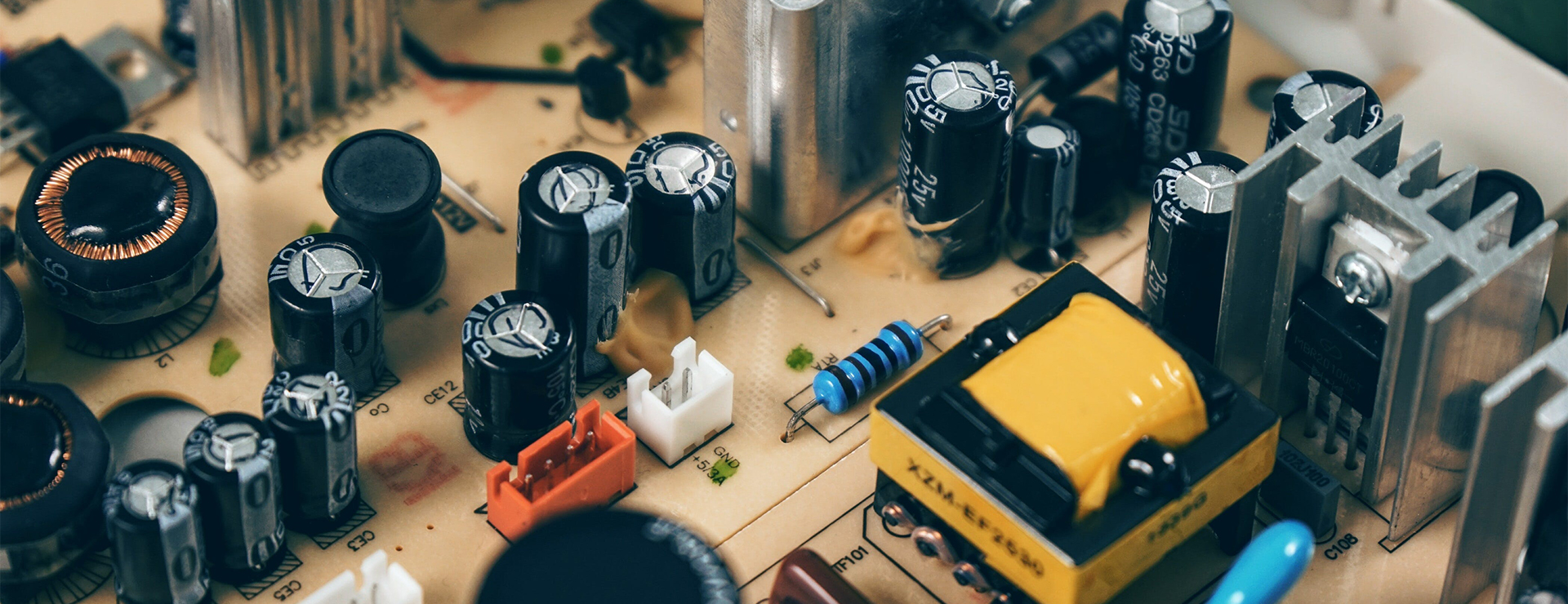


NFC (Near Field Communication) technology has revolutionized the way we interact with digital devices, making tasks such as mobile payments, access control, and data sharing more convenient than ever. In this blog post, we will delve into the applications of NFC tags equipped with Mifare Ultralight chips, highlighting their versatility and potential uses across various industries.

Mifare ultralight nfc tags


What is Mifare Ultralight Chip? Mifare Ultralight is a type of RFID chip developed by NXP Semiconductors, offering a cost-effective and efficient solution for implementing NFC technology. The Mifare Ultralight chip does not require a power source, making it ideal for passive applications where the tag is activated by an NFC reader's electromagnetic field.


Applications of NFC Tags with Mifare Ultralight Chip:


  1. Access Control: NFC tags with Mifare Ultralight chips can be used for secure access control systems in offices, residential buildings, and events. By simply tapping an NFC-enabled device or card on the tag, users can gain entry to restricted areas.

  2. Smart Posters and Marketing: NFC tags embedded with Mifare Ultralight chips can transform traditional posters and advertisements into interactive experiences. Users can tap their smartphones on the tag to access product information, promotional offers, or multimedia content.

  3. Public Transport Ticketing: NFC tags with Mifare Ultralight chips are utilized in contactless ticketing systems for public transportation. Commuters can easily tap their NFC-enabled cards or devices on the tag to pay for fares and access transportation services.

  4. Inventory Management: NFC tags with Mifare Ultralight chips are employed in inventory tracking and management systems across industries. By tagging products and assets with NFC-enabled labels, businesses can streamline inventory processes and enhance traceability.

  5. Event Ticketing and Registration: Event organizers leverage NFC tags with Mifare Ultralight chips for efficient ticketing and attendee registration. Guests can quickly check-in by tapping their NFC-enabled tickets or badges on the tag, reducing waiting times and enhancing the overall event experience.


Unirfid specializes in providing NFC tags, cards, and wristbands with Mifare ultralight chip, offering a comprehensive solution for variaous options.


Related Products: NFC Tags with Mifare Ultralight chip, NFC Cards with Mifare ultralight chip, NFC Silicone Wristands with Mifare Ultralight chip 

Capacitive and resistive touchscreens are two common technologies used in touchscreen devices, each with its own principles of operation:


Capacitive Touchscreen:

Capacitive touchscreens work based on the electrical properties of the human body. They are made of layers of glass coated with a conductive material like indium tin oxide (ITO).


When you touch a capacitive touchscreen with your finger (which is conductive), it disrupts the screen's electrostatic field, causing a change in capacitance at the point of contact.


The device detects this change in capacitance and calculates the touch point. This technology allows for multi-touch gestures (e.g., pinch-to-zoom) because it can detect multiple points of contact simultaneously.


Capacitive touchscreens are generally more responsive and durable than resistive touchscreens. They are commonly used in smartphones, tablets, and other modern touchscreen devices.


Resistive Touchscreen:

Resistive touchscreens consist of several layers, typically two flexible sheets separated by a small gap. The inner surface of each layer is coated with a resistive material, and the outer layers are conductive.

When you press on a resistive touchscreen, the two layers come into contact at the point of touch, creating a circuit. This changes the electrical current running through the screen.


The device detects this change in electrical current and calculates the touch point. Resistive touchscreens typically only support single-touch input.


Resistive touchscreens are less expensive to produce compared to capacitive touchscreens, but they are generally less responsive and have poorer visibility because of the additional layers.


They are commonly found in older devices such as some GPS units, industrial control panels, and certain types of kiosks.


In summary, capacitive touchscreens rely on changes in capacitance to detect touch, while resistive touchscreens rely on changes in electrical resistance. Each technology has its own advantages and is suitable for different types of applications.

As technology evolves, Thin Film Transistor Liquid Crystal Display (TFT LCD) modules are becoming the backbone of digital displays, valued for their sharp resolution, fast response times, and vivid color accuracy. TFT LCDs are widely used across industries, including consumer electronics, automotive interfaces, industrial equipment, and medical devices, making them a versatile solution in today’s digital world.


Understanding TFT LCD Technology

A TFT LCD display is a type of LCD that uses thin-film transistor technology to enhance image quality. This technology arranges pixels in a matrix, where each pixel is individually controlled, allowing for higher contrast ratios and better color depth. Unlike traditional LCD displays, TFT technology significantly reduces “ghosting” effects, making it ideal for applications requiring smooth, high-speed graphics.


Key Components of TFT LCD Modules

TFT LCD modules are crafted with multiple layers. These generally include the TFT glass panel, the backlight unit (BLU), and control circuitry. The TFT layer governs each pixel’s behavior, allowing for fine-tuned brightness and color management, while the backlight provides consistent illumination across the display. This layering creates a vibrant visual experience with precise control over color and brightness, making TFT LCDs a top choice for applications demanding clarity and responsiveness.


Advantages of TFT LCD Displays

Enhanced Image Quality: TFT technology allows for high-resolution displays with vibrant colors and deep contrast, ensuring sharp visuals.

Fast Refresh Rates: Ideal for moving images, TFT modules minimize lag, providing a seamless experience for video playback and graphic applications.

Wide Application Range: From mobile devices and cameras to industrial machinery, TFT LCDs adapt well to diverse environments and uses.


Golden Vision Optoelectronic: Leading TFT LCD Manufacturer

As a one-stop LCD and LCM provider, Golden Vision Optoelectronic Co., Ltd is dedicated to developing and manufacturing advanced TFT LCD modules. Our modules meet international standards and are certified for quality (ISO9001, IATF16949) and environmental compliance (ISO14001, RoHS). With a robust infrastructure and a commitment to innovation, we aim to deliver TFT solutions that cater to both emerging and established market needs.


Choosing the Right TFT LCD Module

When selecting a TFT LCD, consider factors like resolution, viewing angle, and environment. Golden Vision Optoelectronic offers a wide variety of TFT LCD options, customizable to your application’s needs, ensuring both functionality and reliability in any setting.

The environment of an electron microscopy lab does not directly impact the electron microscope itself but rather affects the imaging quality and overall performance. During the operation of an electron microscope, the fine electron beam needs to travel in a high vacuum environment, covering a distance of 0.7 meters (for Scanning Electron Microscope) to over 2 meters (for Transmission Electron Microscope). Along the path, external factors such as magnetic fields, ground vibrations, noise in the air, and airflows can cause the electron beam to deviate from its intended path, leading to a degradation in imaging quality. Therefore, specific requirements need to be met for the surrounding environment.


The Active Low-frequency Demagnetization System, mainly composed of a detector, controller, and demagnetization coil, is a specialized device used to mitigate low-frequency electromagnetic fields from 0.001Hz to 300Hz, referred to as a Demagnetizer.


Demagnetizers can be categorized into AC and DC types based on their working ranges, and some models combine both types to meet different working environments. The advantages of low-frequency demagnetizers include their small size, lightweight, space-saving design, and the ability to be installed post-construction. They are particularly suitable for environments where it is difficult to construct magnetic shielding, such as cleanrooms.


Regardless of the brand, the basic working principles of demagnetizers are the same. They use a three-axis detector to detect electromagnetic interference signals, dynamically control and output anti-phase currents through a PID controller, and generate anti-phase magnetic fields with three-dimensional demagnetization coils (typically three sets of six quasi-Helmholtz rectangular coils), effectively neutralizing and canceling the magnetic field in a specific area, reducing it to a lower intensity level.


The theoretical demagnetization accuracy of demagnetizers can reach 0.1m Gauss p-p, or 10 nT, and some models claim even better accuracy, but this is only achievable at the center of the detector and cannot be directly measured by other instruments due to mutual interference at close distances or the "Equipotential Surface" phenomenon at greater distances.


Demagnetizers automatically adjust the demagnetization current based on changes in the environment. At times, the current can be significant. It is important to pay attention to the wiring layout when other sensitive instruments are in close proximity to avoid interference with their normal operation. For example, electron beam exposure devices have been affected by nearby operating magnetic field detectors.


The power consumption of the demagnetizer controller is generally around 250W to 300W.


The detector of the demagnetizer can be a combination type or an AC/DC separate type, and there is no significant difference in performance. It is generally fixed in the middle-upper part of the column or near the electron gun (as the electron beam emitted from the electron gun may have a slow speed, making it more prone to magnetic field interference). During the initial installation, the detector can be tested at multiple positions to determine the most effective location for fixation.


The demagnetization coils usually adopt a "large coil" design, where six coils are fixed on various walls, ceilings, and floors of the room as far apart as possible. Alternatively, rectangular frames with embedded coils can be customized. However, the "frame" design is less common except for cleanrooms or large rooms. This is because the demagnetization effect is slightly inferior, and it can interfere with the operation and usage of Electron Microscopes.


From the basic working principle of the demagnetizer, the following conclusions can be drawn:


1) Due to the inherent hysteresis that is difficult to eliminate, there will always be a phase difference between the anti-phase magnetic field and the ambient interference magnetic field, limiting the demagnetization effectiveness.


2) In the three-dimensional space enclosed by the demagnetization coils, the demagnetized magnetic field is not uniform. It gradually deteriorates from the center of the detector towards the outer surface, as the magnetic field intensity is inversely proportional to the square of the distance from the signal source (i.e., the demagnetization coils). Moreover, the uniformity of the ambient magnetic field is generally superior to that generated by the demagnetizer, resulting in a reduced demagnetization effect as the distance from the center of the detector increases.


3) This phenomenon particularly affects the use of demagnetizers in Scanning Electron Microscope rather than Transmission Electron Microscope.