Introduction
The digital revolution has brought the Internet of Things (IoT) into the fabric of our daily lives. Wi-SUN technology, celebrated for its robust performance and versatile applications, has become a favored option for large-scale IoT implementations. This article explores the Wi-SUN technology market, its main benefits, use cases and applications, and RF-star’s implementation of Wi-SUN.
Wi-SUN Technology Market
Recent Wi-SUN Technology Market Research Report by Business Research Insight and Market Research Future indicate that the global Wi-SUN technology market, valued at USD 319.27 million in 2022, is predicted to reach USD 14.568 billion at a whopping 13.45% CAGR between 2024-2032. This surge is fueled by ongoing proliferation of smart meters, sensors, and IoT devices, as well as the accelerated digital transformation spurred by the COVID-19 pandemic. Notably, North America stands out as a region with significant adoption of Wi-SUN technology.

Figure1:Wi-SUN Technology Market Size, 2023-2032 (USD Billion)
Source: https://www.marketresearchfuture.com/reports/wi-sun-technology-market-8695
Wi-SUN Overview
What is Wi-SUN?
Wi-SUN, or Wireless Smart Ubiquitous Network, is a wireless communication network based on the IEEE 802.15.4 standard. It delivers a high-performance, low-power, long-range, robust anti-interference, high data throughput, and highly secure wireless communication solution.
As a mesh network, it facilitates long-distance communication and high-data transmission between IoT devices through frequency-hopping and self-configuration technology. The network also features self-healing capability.
Wi-SUN supports two primary operational profiles: Home Area Network (HAN) and the Field Area Network (FAN):
-
HAN: Home Area Network HAN currently has several types, including Router B and enhanced HAN (supporting relay transmission). Router B refers to the Home Energy Management System (HEMS) controller, connecting smart appliances and smart meters. It enables real-time monitoring of smart appliance energy consumption and communication with FAN for smart city applications, enhancing the smart home environment.
-
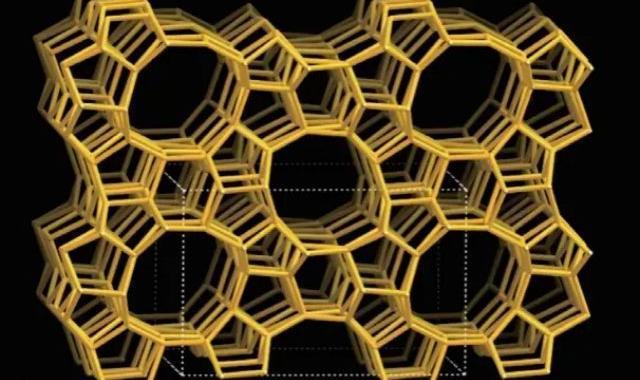
FAN: Field Area Network Wi-SUN FAN is a mesh network where each device can establish multiple connections with nearby devices, scaling up to thousands of nodes. Each node provides typical long-distance hops. If an end-device fails to connect with another, it will automatically re-configure to an alternate path for other end-devices to the router node. This makes it ideal for large-scale infrastructure such as smart grids and streetlights. The Wi-SUN topology is illustrated below:

Figure 2 Wi-SUN network topology
Benefits of Wi-SUN Network
-
Low Latency and High Data Throughput: Wi-SUN’s mesh topology, ensures a low-latency communication experience and supports high data throughput, catering to the demands of large-scale IoT deployments.
-
Low Power Consumption: Wi-SUN devices typically use battery power, significantly reducing energy consumption and extending device life.
-
Ease of Deployment and Scalability: Its straightforward network structure and support for self-forming networks make Wi-SUN an ideal choice for large-scale applications, with the flexibility to expand as the IoT ecosystem evolves.
-
High Security: Wi-SUN offers multiple layers of security mechanisms, such as advanced authentication, to ensure the safety of data transmission.
-
Interoperability: Based on the open standard IEEE 802.15.4, Wi-SUN supports data interoperability between end devices, enhancing overall network efficiency and application coverage.
-
Cost-Effectiveness: By integrating self-forming and adaptive frequency hopping technologies, Wi-SUN reduces overall costs, particularly suitable for in a wide range of IoT applications.
-
Wide Area Coverage: Using radio waves in the Sub-1GHz band (860MHz band, 920MHz band, and other bands below 1GHz), Wi-SUN offers longer reach and less radiofrequency interference with other electronic devices and obstacles. It is ideal for connecting utilities such as smart cities, smart homes, and energy management systems.
Wi-SUN Applications
Wi-SUN technology is finding its place in various global applications:
Smart Cities
Wi-SUN's long-distance transmission, scalability, bidirectional communication, and low power consumption have led to its deployment in many cities for smart meters and streetlights. For example, a Smart Cities Living Lab in Hyderabad, India, utilizes Wi-SUN mesh network technology to manage city assets efficiently.
Smart Streetlights
Wi-SUN technology supports large-scale outdoor IoT networks, including AMI metering and distribution automation, offering smart streetlight solutions for cities. In London, Wi-SUN mesh networks power streetlights, reducing maintenance costs and energy consumption while enhancing flexibility for aesthetic lighting and public safety.
Smart Meters
In smart cities, Wi-SUN technology enables real-time monitoring and management of electricity usage, optimizing energy distribution and reducing consumption.
Solar Power Plants
Wi-SUN networks allow for real-time monitoring of solar panel operations through intelligent monitoring systems, ensuring maximum power generation efficiency while minimizing environmental impact.
Smart Low Voltage Cabinets
In smart grids, Wi-SUN technology is used to deploy smart low-voltage cabinets, dynamically adjusting power supply and optimizing power distribution to enhance grid reliability and flexibility.
Industrial Facilities
Wi-SUN technology is also applied in the industrial and manufacturing sectors, providing non-proprietary solutions that make deployment more scalable, flexible, and secure.
RF-star Implementing Wi-SUN
As a global manufacturer of wireless modules, RF-star can supply a range of Wi-SUN modules based on TI CC1312 and CC1352 series chips.
Key Wi-SUN Modules
-
RF-SM-1277B1: Based on the CC1312R MCU, this low-power wireless module is designed for Sub-1GHz band from 779 MHz to 930 MHz.
-
RF-TI1352P2: Integrating a power amplifier, this module achieves a maximum transmit power of +20 dBm in the Sub-1 GHz band, offering a longer transmission distance and stronger penetration capability. Additionally, RF-TI1352P2 can operate in the 2.4 GHz band.
As shown below, the parameters of the Wi-SUN modules are listed:

Figure 3 RF-star’s Wi-SUN Modules
Upcoming Releases
In August, RF-star is set to launch a new Wi-SUN module based on the TI CC1354P10 SoC. This module is expected to be a multiprotocol and dual-band 800 MHz - 928 MHz and 2.4 GHz wireless module with 1024 kB Flash and 288 kB RAM. Notably, the RF-TI1354P1 module can operate as a border router, extending up to 300 nodes. This will provide robust support for large-scale, distributed IoT complex applications. Stay tuned!
Conclusion
Wi-SUN's unique mesh network architecture, combined with its low latency, high data throughput, low power consumption, ease of deployment and scalability, high security, interoperability, and long-range transmission capabilities, makes it an ideal solution for wide-area large-scale IoT applications. As the market for Wi-SUN continues to expand, its applications in smart cities, smart energy, and industrial IoT are growing, showcasing its potential to enhance connectivity efficiency, reduce costs, and improve user experience. With manufacturers like RF-star leading the development of high-performance Wi-SUN modules, the future of large-scale distributed IoT deployments looks promising.


 Backup Power:
 Renewable Energy Storage
 Uninterruptible Power Supplies (UPS)
 Electric Vehicles (EVs)
 Automotivehttps://www.yeeupower.comMotorcycle:
 Industrial Applications: